- Finding an Application for a New Technology
- Product Definition Challenges
- Device Technology Push for mmW Bands
- 5G UE Devices’ Sensors
- KOKUSHO Patent & IP law firm
- DLL vs. PLL
- What is eSIM?
- Post Design Validation
- What is 6G and when will it arrive?
- What is Startup Company 2nd Challenge?
- Analog vs. Digital Signal Processing
- Startup Companies’ Number 1 Challenge
- What is the relationship between intelligence and imagination?
- How to calculate Exact Number of Bits for DSP Algorithms?
- Design of an Experiment, DOE
- Self-Transmitter Interference Cancellations Feasibility
- What are the differences between AI vs. ASI?
- FMCW vs. Pulsed Radar
- Mobile Wireless Communications Connectivity Between 2020 – 2027
- The Smart City Concept
- What should be Statistical Sample Size?
- Why femtocells are needed and how does it work for 5G?
- The 5G Concept
- Diode vs. MEMS for Beamforming
- Analog vs. Digital Beamforming
- What is LEO SATCOM?
- What are the differences between Lidar vs. Radar?
- Why Antenna Surrounding Matters?
- What are the challenges of radio coexistence?
- What is Radio Statistical Analysis?
- What are 5G Waveform Potential Candidates?
- What are 30 GHz design challenges?
- What is Radio Systems Engineering?
- Who are 5G MODEM SoC players?
- Why Broadcom is trying to buy Qualcomm?
Finding an Application for a New Technology
Every startup company which is introducing a new technology must find an application for their product. The key to their success is to find an application which is not only at least solving a problem, but also it is at additional cost that the market is willing to pay for. This phenomenon exists for every new technology and typically handful of competing startups has a variation of the new technology. The difference between make or break for successful startup company is the product definition which has market traction.
Some startups make the market expectations and become popular after their product is introduced.
Another portions of the startups have partial product, that means, the standalone product by itself will not be viable end user product, yet, with additional features and/or integration can be a viable product. In those cases, the startups are being acquired by bigger and more established businesses for the integration into streamline product. These startups are still successful in returning the investment.
The startups which end on the bottom are the one that their product cannot attract end user or big business for sustainable product. Eventually, they run out funding and go out of business.
Successful products out of new technology are realized by system engineers with business acumen.
Partner with ORTENGA for your product design and development.
Inquiry send to: [email protected]
Posted on December 29, 2018
Product Definition Challenges
In technical industry, any new product definition has a great deal in “make” or “break”, i.e. success in its market.
In other words, the most important contributor of any new product for technical market is its feature sets. Some products come short of having all required features that the market would need at the time of introduction. Other products have adequate features, yet come short of a single and driving feature for many economy valued market, competitive cost.
This is a big risk which is particularly exacerbated for any startup company that relies on a single product to be introduced into the market.
In order to reduce that risk and go to market with competitive product, product definer should acquire inputs from every source that is in her/is disposal. The resources are not only comes from business development for target market and required cost, technical design for feasibility of making the product, but most importantly from systems engineering expertise that looks at product in much bigger context. Specially, if the system engineer has business acumen, it is certainly helpful to capture all inputs from him/er, before settling on the product features.
Partner with ORTENGA to design and develop your new product.
Inquiry send to: [email protected]
Posted on December 20, 2018
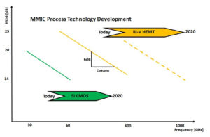
Device Technology Push for mmW Bands
CMOS technology has been the technology of choice for baseband digital and mixed signaling for number of decades. In that past decade, CMOS was utilized for some of RF transceivers.
As radio transceivers go into mmW bands, the use of CMOS for RF signaling becomes limited and III-V compound technology are required to meet the specifications. The following chart illustrates the Maximum Stable Gain, MSG comparison for CMOS vs. III-V compound technologies over the next few years.

Inquiry send to: [email protected]
Posted on December 14, 2018
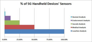
5G UE Devices’ Sensors
The mobile handheld devices are getting more advances year after year. In addition to the datarate and/or speed of the mobile device, there are other peripheral sensors that make them smarter and useful for many applications beside the legacy use.
The following chart shows the estimated percentage of 5G compliant Handheld Mobile Devices’ Sensors.

Inquiry send to: [email protected]
Posted on December 14, 2018
KOKUSHO Patent & IP law firm
The consultancy service for inventors (typically provided by patent attorneys) for enhancing technological level of their ideas (brushing up their invention) is important but some renewal is required with respect to the consulting methodologies for such purpose. We have researched traditional approaches such as TRIZ, Mind Map and KJ method and found that novel approach is required for simplifying the technological analysis while making easier to achieve the effective brushing up of the invention. More specifically, such approach for invention brushing up should be more straight forward and can be directly applied to the inventions conceived for filing patent applications.
For more detail, refer to the link below.
The new approach is innovative in the following respect.
(Phase-1): First, brushing up is performed on theoretical fundamentals such as mathematic modeling or mathematic formulation to establish the enhanced or strengthened version of theoretical fundamentals (for example, optimizing a style of mathematic modeling so as to best fit to the problem domain the client’s invention attempts to deal with).
(Phase-2): And then, on the basis of the enhanced or strengthened version of theoretical fundamentals (such as the further optimized version of mathematic modeling) as mentioned above, engineering level improvements such as technological enhancements or technological improvements are made in the engineering aspect (in view of engineering application or industrial application of technology) of the client’s invention.
Thus, according to our novel approach, the technological level of the invention can be much further elevated, in comparison to that of the conventional approach. Such advantage of our novel approach can be achieved by making the technical enhancement or improvement in the level of engineering application on the basis of the enhanced or improved version of the theoretical modeling or the theoretical formulation.
As a result, some kind of breakthrough can be achieved in terms that our novel approach can surpass the upper limitation of invention brushing up that the conventional approach can never overcome.
Inquiry send to: [email protected]
Posted on December 11, 2018
DLL vs. PLL
Delay-Locked Loop, DLL, and Phase-Locked Loop, PLL, are used to phase lock an output to an input signal source.
DLL consists of delay line, multiplier, LPF, and feedback, whereas PLL consists of multiplier, LPF, VCO, and divider feedback.
The sources of added phase noise are multiplier and delay line for DLL, whereas in the case of PLL, in addition to multiplier and divider, the VCO is also source of added phase noise.
Therefore, DLL has better phase noise performance and lower sensitivity to supply noise.
DLL is meant for phase-locked in the baseband, whereas PLL can be used in the radio front end and the output could be much higher frequency than input signal.
Both DLL and PLL are used for carrier tracking and synchronization.
Inquiry send to: [email protected]
Posted on December 10 2018
What is eSIM?
The electronic Subscriber Identification Module, aka, eSIM is new provisioning technology to configure and enable HW/SW of a mobile device before it can connect and be used with local carrier or service provider.
SIM is a legacy technique that enables phone and mobile devices for a particular region/geography under a carrier/service provider. However, it falls short of providing global coverage when you decide to travel, unless you physically replace one SIM card with another.
Major carriers are looking into eSIM to enable their customers with global mobile device and harness additional business by partnering with distant carriers.
Partner with ORTENGA to find out eSIM techniques.
Inquiry send to: [email protected]
Posted on December 3 2018
Post Design Validation
In the fast growing and changing consumer market, the need for validating design in few months has become the difference between high vs. low margin or even business opportunity at all for many manufacturers.
Traditionally, the product development teams make a list of features and metrics that they like to be tested in post design phase. With the advancement and sophistication of many technologies, to verify that complete list, it will take months if not a year to exhaust all possible features and metrics of the product.
The traditional post validation technique is based on the Black Box assumption. In other words, the validation team treats all the features and metrics equal in risk table. That is saying the probability of any of the features and metrics failing during the test is equal, hence uniform failure rate. That is erroneous assumption which cost the company resources and time to market, TTM. Estimating resources or TTM wrong, it is either low or no margin at all.
Successful companies, the one which introduce their product to market first without issues, utilize Design of Experiment, DOE methodology. The DOE is realistic about the probability of failure and does not assume uniform failure rate.
For instance the phone, UE, ODM industry releases 2 phones per year, one in June and the other in December. June release requires December SoC, RFIC, PMIC, and ASIC production readiness. This is well known to all vendors and they pretty much starts developing competing technology at the same time. Some are able to make it before the deadline and others miss that, and the difference is the methodology for validating the design.
Partner with ORTENGA in your product design and development.
Inquiry send to: [email protected]
Posted on November 30 2018
What is 6G and when will it arrive?
Wireless industry visionaries are already talking about 6G, even though 5G has not launched. From the outset, it sounds like hypes than anything realistic and it may very well be not materializing the way it appears now. In spite of that, let’s put on the same goggle and walk in to future and see what is there.
So far, every generation of wireless communication standards were based on increasing the capacity and speeding up the network connectivity. With 5G around the corner, we would reach the limits of what is tangible to human in terms of speed. Capacity would reach to similar limit that we human won’t be able to process faster than what is available to us.
6G will be a paradigm shift from HW/FW/SW requirements to actual applications. In other words, 6G will be defined at the Application Layer and would work its way down to NET, MAC, and PHY layers. Although some changes will be required for NET, MAC, and PHY layers, they would be incremental and not significant compare to 5G. What would be significant about 6G, is that the applications will be much user friendlier and with significant capable artificial intelligent UE. You will not need to type for interfacing with your devices, merely talk to device or even simple jester would do work.
AI of voice activation and jester recognition are under way by many companies and devices are being design and developed already. One could claim that s/he is working on 6G already, and that would not be far from truth.
With the current implementations of AI and ASI, a good estimate would be 2027 for fully 6G devices and applications.
Partner with ORTENGA to succeed in your product design and development.
Inquiry send to: [email protected]
Posted on November 29, 2018
What is Startup Company 2nd Challenge?
In order to run successful technology startup, the head of engineering team, either CTO and/or VP of Engineering has to be truly committed to the technology and the first believer of the product, s/he is developing. Any lack of commitment would be picked up by managements consequently engineering teams. Effectively at the least, it slows down the progress and deliverables’ time line, or creates an atmosphere of void execution within the organization with respect to its true and meaningful potentials.
Startups are supposed to be bold in taking risk on a single technology. In other words, they have only one product, and have to be first in getting that product to the market to surpass any other competitor. In order to do that, startups are supposed to be quick in vetting their options and making decisions on daily basis which has significant impact on their survival. This is high stake and risky business and development plan and any failure is catastrophic. That is the nature of startups.
In contrary, a well-established company has large number of products, portfolio, and resources which can afford missing some opportunity without going into red zone, yet they are slow in implementing any new technology because of lengthy and vetting process by which large numbers of stakeholders decide and typically not the first in disruptive technology.
The startup’s engineering leadership must be transparent and on-board with the same level of belief for disruptive technology which they are developing as the founder(s), not just by echoing the company’s goal in their statements, but with their behavior, action, and unwavering commitments dealing with engineering managements. Anything less than that; would lengthen the development timeline and diminish any ROI if not all.
Partner with ORTENGA to succeed in your product design and development.
Startup Companies’ Number 1 Challenge
Inquiry send to: [email protected]
Posted on November 25, 2018
Analog vs. Digital Signal Processing
The world around us is analog, e.g. light, sounds, smell, temperature, etc.
In fact, all sensors around us are also analog in nature.
However, it is advantageous to convert the analog information into digital using analog to digital converters, ADC, and process the information in the digital domain.
By converting the analog to digital signal and perform the processing in the digital domain, there are 3 fundamental benefits.
- Digital signals are more tolerant to noise and/or distortion. In technical terms, digital modulations require lower signal to noise ratio before detection.
- Digital signals require less of frequency spectrum. In technical terms, digital signals increase capacity, i.e. more users per frequency spectrum.
- Digital signals are more secure. Once the analog signal is digitized, it is very easy to encrypt them. The encryption can be changed on the fly to new codes, if it is compromised.
Because of the above, nowadays any analog signal is digitized using ADC and processed in digital domain via microprocessor.
There are additional benefits that comes by digitizing the signal of interest, namely; it can be stored and retrieved easier. Digital signals can be encoded to decrease required signal to noise ratio before detection. The semiconductor processes in which handles digital signals are more robust to manufacturing tolerances and yield better, therefore lower cost per square area. The semiconductor is also requires less or no calibration prior using operating the device, i.e. less cost for bring up.
The benefit list goes on.
Future technology will rely on high speed broad bandwidth ADC and DAC and limits the analog medium to the air interface channel, antenna, LNA and PA in radio communications. Everything else will be handled in the digital domain which can be manipulated via SW, hence Software Defined Radio, SDR.
Inquiry send to: [email protected]
Posted on November 16, 2018
Startup Companies’ Number 1 Challenge
In good and healthy economy, many startup companies get funded and start developing proof of concept innovative technologies. In technology industry, the number one challenge for these companies is to realize an actual product for the new technology that they have designed and developed. In other words, which product is worth continue developing in order to make good on the return of investments. The challenge comes about that any new technology has at several opportunities to be harvested upon. Each opportunity requires dedicated resources and different time to market time line to arrive at end user product. The startup company does not have the means and resources to invest resources in each single opportunity, therefore it has to take risk in selecting one or maybe two opportunities partially and wait for reaction from the market. By the time the market reacts, if it is not too late to change direction for market traction, the startup would be out of funding. To overcome this challenge the market has to be well understood before making any commitment to the product on the roadmap. The understanding of the market requires evaluating internal capabilities vs. external future demands. Both of which are not only requires technical know-how but also business acumen with vision for the market. Most startups have either technical or business product owner who makes the call, but not both. The end product is either technically fit, yet does not meet cost and customer feature targets, or too broads in frivolous features without topping legacy technology in any particular aspects.
Partner with ORTENGA to succeed in your product design and development.
What is Startup Company 2nd Challenge?
Inquiry send to: [email protected]
Posted on November 14, 2018
What is the relationship between intelligence and imagination?
Intelligence is the act of processing knowledge and/or information to draw conclusions to benefit a desired outcome. Every human being, or being, has intelligent to certain degree and using that on daily basis.
For instance, when you arrive at any new city and would like to reach your particular destination, you use the information about the geography of that city, where about of your destination, public or private transportation schedule and availability to plan the timing, cost, and schedule that makes sense for you. This process is demonstration of your intelligent at work to arrive at your destination.
In regard to Artificial Intelligent, AI, a machine will be programmed to predict human behavior via an engineered algorithm. For instance, any voice activated Edge Device, such as Alexa or your Smart Phone, will listen to your instruction or question to come up with pre-programmed response to satisfy your need. Again, this is machine reaction to your instruction or question is AI at work.
On the other hand, imagination is seeing beyond routine behavior or typical response for given situation. For instance, in 1960’s Star Trek TV serial, envisioned a “handheld wireless foldable pocket size communicator” that could be used to communicate between Star Trek’s crews or officers. We now see that “communicator” has been realized in late 1990’s by Motorola original flip mobile phone. This is imagination at work.
Mathematically, intelligence is interpolation between available data points to draw conclusion, whereas imagination appears to be even further than extrapolations.
Imagination is extremely difficult to teach, if not impossible, yet alone being programmed to any machine.
Share your view via: [email protected]
Posted on November 11, 2018
How to calculate Exact Number of Bits for DSP Algorithms?
Digital Signal Processing, DSP, algorithms are typically coded in MATLAB with floating point numbers. Whereas the implementation of the same algorithm in HW/FPGA is bounded by limited number of bits, therefore, there is question of how many bits are actually required such that the given algorithm has adequate accuracy.
The short answer is that the exact number of bits can be analytically calculated similar to ADC or DAC’s ENOB and it can be validated via fixed point in MATLAB to ensure the exact number of bits produce the expected accuracy.
This is the link to ADC and DAC number of bits calculation for 5G examples.
Inquiry send to: [email protected]
Posted on November 3, 2018
Design of an Experiment, DOE
In 1950’s Japanese car manufactures were facing the fundamental manufacturing problem, namely; how to make cars with adequate yield. In other words, every car which was produced was not necessarily reliable or working properly as expected, i.e. yield was low.
In order to solve the problem, the engineers became aware of car manufacturing process issues and had to find which part of process impacts what output quality parameters. The issue was that there were too many parameters to deal with and correlating back to root cause, process step, was tedious, expensive, and would take months if not years to sort out.
The car manufacturer hired a consultant, W Edward Deming, to look into issue, someone with fresh ideas, outside of the box. During this time a Japanese engineer, Taguchi, discovered and documented statistical techniques to design experiments that are orthogonal and provides significant information which can be utilized to correlate the issues back to it process source.
Nowadays, successful manufactures target 6 sigma processes after running series of DOE during characterization of their products to arrive at adequate yield in high volume manufacturing.
Inquiry send to: [email protected]
Posted on October 26, 2018
Self-Transmitter Interference Cancellations Feasibility
Typical communication radios utilize frequency and/or time division diversity for two way radio communications. This is to ensure proper operation of receiver in the presence of a very loud transmitter. In other words, while the transmitter is talking, the radio can’t receive in the same frequency band at the same time, due to self-interfering/jamming of the receiver. This is even true for, human voice communications, at least for most of us if not all that; we can’t talk and listen at the same time.
There is an interest to be able to talk and listen at the same time in any radio. It saves frequency spectrum and/or time. The spectrum cost us more than $500/Hz, whereas lost time is not even replaceable, therefore there is research going on to realize a radio that can transmit and receive over the same frequency band simultaneously.
The problems to be solved are three folds, first the dynamic range of the required receiver, second the accuracy or tolerance of required hardware to realize such a radio, and third maintaining the self-transmitter cancellations over a wide bandwidth.
There are number of techniques to assist the receiver in cancelling self-transmitter interference while both transmitter and receiver are operating, namely; digital cancellation, analog cancellations either via phase, vector modulation, or signal inversion.
Inquiry send to: [email protected]
Posted on October 22, 2018
What are the differences between AI vs. ASI?
Artificial Intelligent, aka AI, consists of sensor/HW, FW, and SW which can predict the outcome of a particular event, via utilizing prior algorithm. Typically the algorithm has to take into account some human and/or machine behaviors. The sensor takes the data of present, the algorithm compare the current data against the previous history and predict the outcome an event. The algorithm could be residing in FW and/or SW.
Many, if not all, high technology companies have AI division; to name a few: Amazon, Apple, BMW, Daimler Mercedes Benz, Facebook, Google, Microsoft, Nvidia, Qualcomm, Samsung, Tesla, Toyota, and Volkswagen.
For instance, any voice recognition algorithm can be considered AI. The voice AI is supposed to understand and/or predict the verbal/voice instructions.
Any face recognition algorithm can be considered to be AI. The face recognition AI is supposed to map the face of an individual to all known identity in its history or library.
Any grocery marketing algorithm can be considered AI. The grocery AI is supposed to predict the grocery items that you potentially purchase and provide you with marketing information, such as coupon, discount, particular vendor, available locations, etc.
Radio front end algorithm which can sense interference/unwanted signal and adjust gain and linearity, aka cognitive radio, of wireless system front end can be considered AI.
Artificial Super Intelligent, aka ASI is the combination all of the above. ASI consists of multiple sensors, FW, and SW which can predict human behavior based on previously trained human models and algorithms. ASI also has capability of making predictions outside of prior algorithm, once it has statistical data and behavioral model.
Inquiry send to: [email protected]
Posted on October 16, 2018
FMCW vs. Pulsed Radar
Radio detection and ranging, aka radar, was invented to detect and estimate military target range before WWII, 1930’s. Originally this was done by transmitting a Continuous radio Wave, CW or sinusoidal, and listening to the echo bouncing back from the target of interest. The echo signal intensity would be compared to clutter, noise level of the receiver, and if above certain threshold, it would indicate the existence of the target, i.e. detection. The bigger the target, aka radar cross section/RCS, the stronger the echo signal is. The echo signal would also be shifted in frequency, aka as Doppler shift. The Doppler frequency shift, frequency modulated CW/FMCW, is proportional to radial speed between radar and target. The Doppler shift is negative relative to the CW, if the target is going away and positive if it is heading toward the radar.
During WWII, radar became extremely important and the race started to improve it by increasing the radar range that could detect a target. This proved to be challenging as additional range meant much higher power, in fact by x4. In other words, to double the radar range the transmitted power have to be increase by 16 times. There were two problems, the obvious limitation of transmitted power and its security. The stronger the transmitted power of the radar, the more obvious to be detected itself and be neutralized.
The advance of electronic technology and digital signal processing algorithms enabled optimizing the required transmitted power and acquire additional information about the target, Pulsed radar was invented. The pulsed radar provides better time stamp of the target by compromising the frequency information/speed resolution.
Nowadays, advanced radar can provide both accurate time and frequency of the target signature with what is known as Pulse Compression Radar. Pulsed Compression Radar modulates pulses to optimize both range and speed of the target, while maintaining the transmitted power.
Current radars can tell much more information about the target, such as; radial speed, direction, size, track, and even identify the target.
Radar has found its market in commercial application and will be important feature of autonomous car, Positive Train Control/PTC, and auto pilot airlines.
Inquiry send to: [email protected]
Posted on October 6, 2018
Mobile Wireless Communications Connectivity Between 2020 – 2027
Many clients ask about the mobile wireless communication outlook in various contexts. The questions are typically around 5G and its user experiences. The following graph summarizes what we are about to experiences for mobile connectivity for the next several years.
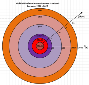

The user equipment, UE, the mobile device will have capability to sense and connect to the optimum mode of operations depending on its location and availability of network. The handoff will occur on the fly, with the only exception of LEO SATCOM Connectivity.
In brief, for very short distances, BT/802.15 will be used for data transfer as it is today, with some tailored improvement for datarate and power consumption. This is basically device to device, d2d, connectivity.
For local area, such as home or office, 802.11xx and/or femtocell will be the dominant mode of operations. Depending which transceiver you have, the datarate will be about ~7Gbps. If you don’t have any WiFi, equivalently, femtocell can be utilized instead and datarate will be about ~5Gbps.
Once you step outside of your home and office yet still in urban area, the UE will be connected to gNB or eNB depending on the availability of network, with associated datarate between 1 – 10 Gbps.
In remote areas, User Terminal, UT, the LEO SATCOM will be available to keep connectivity with 100Mbps datarate. It is possible that the UT would be dual purpose and acts as UE as well.
Inquiry send to: [email protected]
Posted on October 4, 2018
The Smart City Concept
The Smart City concept has been taking shape for the past 5 years.
The concept is intelligent connectivity between commercial and public facilities to your handheld device, UE.
As you walk in downtown area, you will be able to access information regarding restaurants, bus or train schedules, post office, etc. at your request with much more user friendly applications. You will be able to ask question of your UE and the response will pop up or voice to tell you about your destination, the ratings, wait time, menu, etc.
If you have a destination via train, your UE will make you aware of timeline, location, and other options to get you there, think of like Uber, Lyft, Amtrak applications are combined with much more info and extremely easy to use.
Currently, Barcelona is number 1 smart city, followed by Munich.
Inquiry send to: [email protected]
Posted on September 26, 2018
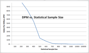
What should be Statistical Sample Size?
Any practical design that makes it to production gets to be tested for quality by end users.
Successful manufacturers have estimate of what portions of their “Good” may Fail, the Escape, consequently becoming the Returned, RMA, by the end users.
For large volume consumer products with low margin, or even for mid margin, it is necessary to validate the RMA quantity to meet cost targets. In other words, the design and quality teams have estimated the number of RMA for Escaping “Good” criteria. The RMA is part of unit cost calculation and target margin and bottom line in the business plan.
The validation process of RMA requires statistically testing several units and determines the number of Defect per Million, DPM, for that product. The questions become how many units should be tested to acquire enough information about the high volume product.
The larger the sample size, the higher confident is gained with higher price tag for larger scope of testing, time, and efforts. Obviously, manufacturers would like to test as few as units, yet still estimate DPM and validate their cost model.
The following is an example of this analytical process to control the statistical sample size.

ORTENGA can analyze your product statistical behavior.
Inquiry send to: [email protected]
Posted on September 25, 2018
Why femtocells are needed and how does it work for 5G?
5G mmW have significant attenuation/loss when passing through walls and/or glasses. Therefore, 5G femtocells will be utilized to reach 5G UE within enterprises and homes, see below.

When you arrive at work or home, your 5G phone, UE, will register and authenticate with the local 5G femtocell. This femtocell is connected to your home modem, internet provider for instance, and reports your location. Now any incoming or outgoing calls/data transfer will be handled through the internet to 5G backhaul and routed toward appropriate 5G Fronthaul.
5G femtocell will be less than 1W radiated power and target cost of couple of hundred dollars.
Inquiry send to: [email protected]
Posted on September 24, 2018
The 5G Concept
The wireless industry has been developing 5G Standards for some times now and 3GPP 5G NR release 16 will be available soon. In spite of that, there are some confusion of its implementations and how to reach the end user, UE.
Some manufactures focus on sub 6 GHz, while others go into mmW 28 and 39 GHz spectrum. There is also confusion of how higher spectral efficiency, hence higher throughput will be achieved indoors, urban, rural, or even global remote areas.
It is cost and ROI which will lead to pragmatic solutions.
Here is my view of what is happening.
For urban area, mmW technology will be utilized for venues such as football stadiums, outdoor concerts, downtowns, and some golf courses.
For indoor venues, 802.11ax, 802.11ac, and/or femtocell will be utilized.
For device to device, d2d, handshake and data transfer, 802.11ad will be utilized.
For global remote area, LEO SATCOM will be utilized.
The 5G UE will be able automatically switch/hand off between the above platforms to optimize the user experience for throughput, latency, power consumption, and cost.
Partner ORTENGA in the product design and development before executing your business plan to capture 5G Wave market share in 2019.
Inquiry send to: [email protected]
Posted on September 20, 2018
Diode vs. MEMS for Beamforming
Diodes
Diodes are typically discrete components which can be off the shelf in realizing variable capacitors while they are reverse biased for many applications including RF resonators. Integrated diodes are technically feasible with additional cost of Silicon mask and fabrication facilities for larger scale. The current leakage increases with temperature and impact the capacitance.
MEMS
MEMS can be discrete or integrated into PCB, which has lower fabrication cost and turn around time relative to Silicon. The MEMS have better power handling and lower leakage current.
Overall, for large scale (100 or more) antenna array, integration, switching speed, process stability, and cost are prime considerations in choosing the appropriate component.
Inquiry send to: [email protected]
Posted on September 19, 2018
Analog vs. Digital Beamforming
ABF
In Analog Beamforming, the amplitude and phase shifting occur in RF front end, hence in analog domain. Therefore, due to analog nature, in order to account for performance of amplitude and phase over frequency, temperature, voltage, and process (i.e. part to part), extensive characterization and meticulous calibration algorithms have to be done during the production phase, in addition to careful design topology.
DBF
In Digital Beamforming, the amplitude and phase shifting occur in digital baseband. Therefore, there is no need for production calibration, due to maturity of digital process. This advantage does come at a price of additional DC power consumption for baseband IC.
HBF
In Hybrid Beamforming, the coarse amplitude and phase shifting occurs in analog domain, whereas the fine-tuning happens in digital domain. The HBF are feasible for very large antenna arrays, where ABF and DBF fail to scale due to complexity or power consumption, respectively.
To select proper beamforming topology, careful analysis of use cases as well as complexity vs. power consumption trade-off analysis should be made to down select undesired customer limitations.
Inquiry send to: [email protected]
Posted on September 18, 2018
What is LEO SATCOM?
LEO SATCOM stands for “Low Earth Orbit Satellite Communications”, see below.

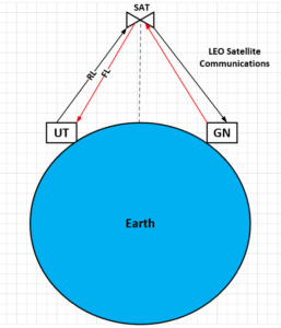
LEO satellites will be launching in 2019Q2 and will be operational in 2020Q2.
LEO is newer technology in comparison to GEO, Geostationary Earth Orbit, and requires less power, smaller size, while providing higher throughput/spectral efficiency.
To date, there are 26 companies making, User Terminals/UT, Satellite, Ground Network/GN products for LEO applications, excluding their vendors.
Significant venture capital is spent supporting many start-ups to capture this new SATCOM market.
Inquiry send to: [email protected]
Posted on September 17, 2018
What are the differences between Lidar vs. Radar?
Radar is an acronym for “Radio Detection and Ranging”.
Radar illuminates a target via radio waves and listens to the echo for acquiring information about the target.
Nowadays, radar is much more advanced technology and also detects the target radial speed, direction of arrival, type, and its size.
Originally, radar’s technology was intended for military applications and over time it has find its way to commercial applications.
Recently, radar’s technology is being designed and developed for autonomous car, train, and plane industries.
Radar’s range could be as short as 100 m up to 250 Km.
Lidar stands for “Light Detection and Ranging”.
Lidar uses Laser/Light instead of radio waves and can depict good resolution picture of the target.
Lidar are for much shorter range of the target, 100 – 150 m.
Nowadays, both Radar and Lidar use sophisticated digital signal processing techniques and algorithms to acquire significant information about the target of interest.
Inquiry send to: [email protected]
Posted on September 17, 2018
Why Antenna Surrounding Matters?
Antenna performance not only depends on its design topology but also on the surroundings which impacts antenna impedance in real world application.
In other words, if one were to design an antenna and meets all its required performance in standalone condition, then when it is embedded with other radio components, the antenna behavior would change, either over frequency or for worst.
In fact, mobile handset antennas are tuned with human phantom after fabrication, to adjust tuning elements in such a way that meets requirements in presence of the human body.
More advanced mobile handsets have capability of adjusting the tuning elements on the fly to account for various surroundings and still meets acceptable antenna performance.
Very advanced mobile handsets have capability of adjusting impedance and aperture tuning elements on the fly.
Inquiry sent to: [email protected]
Posted on September 14, 2018
What are the challenges of radio coexistence?
It is well known that in radio design and baseband frequency planning is a critical aspect of the design to ensure unwanted spurious and/or non-discrete signals generated within the radio, do not harmfully impact the SNR in anyway.
The problem is even more challenging when multiple radios coexist within the same system; for instance, when BT and WiFi are supposed to coexist in the same vicinity or PCB.
Every time you add another radio to the system, your design must take into account precautions such that addresses/mitigates radio coexistence.
In fact, if you were to look up manufacturers such as Apple, Amazon, or Nvidia, they have assigned engineers to deal with just that one issue in their design.
Partner with ORTENGA for design and development of sensitive radios.
Inquiry sent to: [email protected]
Posted on September 13, 2018
What is Radio Statistical Analysis?
External Constraints
Radio design deals with many external constraints, such as unwanted signals from other users (in the same band, IB) or applications (i.e. outside of the band, OOB) which are random and could take many different values.
Internal Constraints
Also, the radio has to perform over some internal constraints, such variation over process (device to device variations), voltage temperature, aka P.V.T. By definition, the radio covers certain frequency band of interest; therefore it has to perform over the frequency band.
A good radio design is robust enough that could perform well both over external and internal constraints.
This requires a statistical analysis to understand the yield (cost of radio) vs. robustness of the radio.
ORTENGA can partner with you to perform statistical analysis on your radio.
Inquiry sent to: [email protected]
Posted on August 31, 2018
What are 5G Waveform Potential Candidates?
Legacy 4G waveform is OFDMA. Although OFDMA has attributes which are interesting for 5G, yet lacks required spectral efficiency to achieve 5G traction. Therefore 5G R&D communities have developed derivative of OFDMA to achieve better compliance with 5G requirements. There are 4 competing 5G Waveforms, namely;
- Filter Bank Multi Carrier, FBMC
- Generalize Frequency Division Multiplexing, GFDM
- Orthogonal Time Frequency Spatial, OTFS
- Universal Filter Multi Carrier, UFMC
5G Considerations Metrics
PAR
Peak power to average ratio, PAR is critical metric which impact PA linearity, consequently PA efficiency. PA linearity and efficiency are two competing metrics and can’t be optimized at the same time.
Spectral Regrowth
As the PA gets close to compression, the spectral regrowth reach out of emission limits set forth by FCC and ETSI. Spectral regrowth impacts adjacent and alternative adjacent channels which belong to another user and shall not be polluted.
Spectral Efficiency
5G KPI is spectral efficiency and whichever waveform utilizes the BW better has good chance of being chosen.
Phase Noise
As the operating frequency increases into mmW band maintaining phase noise becomes more challenging. Given m-ary modulation, the required phase noise is determined. Higher spectral efficiency requires higher m-ary modulation, which translates to better phase noise.
Latency
The 5G Waveform will be a trade-off between spectral regrowth and length of baseband filter (latency).
Interference Immunity
The 5G Waveform will be a trade-off between spectral efficiency and orthogonality (complexity of Rx architecture)
Inquiry sent to: [email protected]
Posted on August 29, 2018
What are 30 GHz design challenges?
At 30 GHz, the wavelength is 1 cm, 0.4 in. Any component in size that is in order of 1/8 wavelength, 1.25 mm, or longer will not only impact the magnitude but also phase of the electromagnetic waves. In other words, SMD inductor and/or capacitor can’t be used and have to be realized via short and/or open stub, aka distributed elements, i.e microwave design.
RF power is premium even more at 30 GHz.
In Tx chain, therefore power loss in transmission line is less tolerable compared to sub 6 GHz. Thus, every component has to be tightly placed on the PCB. Due to proximity, the new challenge becomes required isolation between all these tightly placed components. The mitigation is to understand the electromagnetic method of coupling and avoid them on the PCB, i.e. microwave layout design.
As the frequency goes above 30 GHz, these issues are more pronounced and requires delicate and meticulous design to be have a successful product.
Inquiry sent to: [email protected]
Posted on August 27, 2018
What is Radio Systems Engineering?
Radio systems engineer are responsible to review and capture overall radio requirements. The radio requirements could be divided into two major categories, Air and MODEM interfaces. Any radio design has at least two Systems Engineers, one for Air Interface, who is called Radio Frequency Systems Engineer, aka RF Systems Engineer, and second is Communication Systems Engineers, aka CommSys Engineer.
Air interface refers to the medium in which transmit and/or receive antennas of the radio operate in.
MODEM interface refers to baseband digital signal which has to be processed, via DSP, to decipher digital data after correcting errors incurred during the transmission and produces sent information for the radio user.
RF Systems and CommSys Engineers work together to decompose the Air and MODEM interfaces requirements.
In particular, RF Systems Engineer decomposes and defines every single block from Antenna down to A/D and D/A up to Antenna for Rx and Tx chains of the radio, respectively.
The CommSys Engineer decomposes and defines every single block inside the MODEM from synchronization, AGC algorithm, decryption/encryption, demodulation and modulation of Rx/Tx chains of the radio, respectively.
ORTENGA has seasoned systems engineering team who have previous industry design for supporting your radio project.
The following block diagram illustrates top level block diagram of any modern wireless digital communication systems.

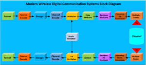
The Channel represents the Air Interface in the above block diagram.
Inquiry sent to: [email protected]
Posted on August 26, 2018
Who are 5G MODEM SoC players?
Qualcomm 5G MODEM
X50 is Qualcomm 5G MODEM which is not only backward compatible with previous mobile Standards such as 4G/LTE, 3G/CDMA, but also supports 802.11/WiFi, 802.15/BT, and GPS/GNSS applications into the single SoC. This is by far the most integrated 7nm TSMC baseband chip for Mobile applications.
Intel 5G MODEM
XMMTM 8060 is Intel 5G MODEM which is backward compatible with 4G/LTE, UMTS, and 2G/GSM mobile Standards. It is based on 7nm Intel CMOS process.
Samsung 5G MODEM
Exynos is Samsung 5G MODEM which is backward compatible to 4G/LTE and 3G/CDMA mobile Standards. It is based on SEC 7nm SEC CMOS process. It is also unclear whether it supports any other mobile technology besides wireless mobile applications.
Media Tek MODEM
Helio M70 is Media Tek 5G MODEM which is 5G and 4G/LTE supporting sub 6GHz Band. This chip is tailored to meet CMCC, NTT Docomo, and Huawei carriers and value tier markets. It is based on 14nm CMOS process.
Apple 5G MODEM?
Apple has been working on baseband chip for the past 5 years, however it is unclear the amount of success in breaking into the mobile MODEM chip technology.
Inquiry sent to: [email protected]
Posted on August 19, 2018
Why Broadcom is trying to buy Qualcomm?
Let’s rewind to view the background of Broadcom. Broadcom originally was founded and succeeded to be the company in infotainment industry with RFIC and MODEM SoC for TV and STB for broadband applications. The success increased the need for growth beyond and into cellular industry in early 2000. Broadcom came close, however could not penetrate the competitive cellular market. Avago ceased the opportunity to acquire Broadcom when it was not growing and in management turmoil. Avago have PA and front end component for cellular market and kept Broadcom name.
Fast forward to current time, Qualcomm is preparing to launch X51/2 MODEM and integrated RF front end, GaAs PA modules with CMOS drivers, Power Management IC, Clock Management IC, all tailored for 5G market. Just the PA modules introduction will hurt Avago/Broadcom bottom line, moreover, it will solidify Qualcomm on its core technology for up to 7 years.
Broadcom acquisition of Qualcomm for purchase price $105B, is no brainer without risk.
Qualcomm front end market worth ~$20B, MODEM SoC is another ~$30B, QTL is estimated to be ~$50B. Other assets such as 30K+ engineering resources, its largest assets, real estates, equipment, and investments worth well over the remaining $5B by ~10x.
It is no surprise that Broadcom has increased the stake and pursuing the acquisition by any means. Whether Broadcom succeed in its acquisition, remains to be revealed in 2018. One thing is clear though if Broadcom acquires Qualcomm, the quickest to make good on that investment, cashing out, is to sell QTL and reduce the engineering resources which supports that business and continue with cellular legacy and 5G for years to come.
Inquiry sent to: [email protected]
Posted on January 9, 2018