ASIC Engineering Realizations — From Semiconductor Architecture to Product Reality
ORTENGA supports ASIC engineering programs across RF, analog,
mixed-signal, digital, baseband, AI, radar, wireless infrastructure,
SATCOM, and next-generation semiconductor-enabled platforms.
We help organizations translate deployment realities, system constraints,
manufacturable hardware realization, and market objectives into executable
ASIC architectures and validated semiconductor-system outcomes.
System Before ASIC.
Architecture Before Tapeout.
Validation Before Scale.
Early Architectural Risk
ASIC failures are often not silicon failures.
They originate from misdefined system assumptions,
architectural boundaries, deployment constraints,
or incorrect subsystem partitioning decisions.
Many semiconductor programs encounter challenges long before fabrication begins.
The root cause often appears during early architecture development,
when deployment assumptions, subsystem boundaries,
operating constraints, manufacturability realities,
or integration expectations are not correctly defined.
ASIC Realization Across System Architecture
Every radio and radar system fundamentally contains four major functional domains:
- Antenna System Module (ASM)
- Front-End Module (FEM)
- Transceiver Module (TRM)
- Baseband Module (BBM)
ASIC realization may exist within ASM, FEM, TRM, BBM,
or across multiple domains simultaneously,
depending on architecture objectives, deployment requirements,
integration strategy, performance targets,
manufacturability constraints, and market positioning.
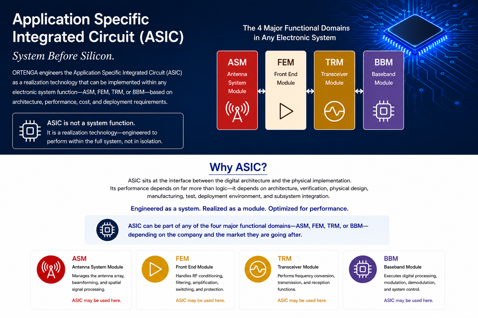
ASIC is not itself a system function.
It is a realization technology engineered to operate within
the larger deployed system architecture.
Realization and Deployment Risk
Functional silicon does not guarantee product success.
ASIC product success depends on whether the semiconductor architecture
remains aligned with deployment realities,
subsystem interaction,
integration constraints,
manufacturability,
validation requirements,
and market objectives.
Technical implementation success can still drift away from product realization.
Semiconductor programs may function technically while failing to gain meaningful
product traction if architecture decisions drift away from deployment realities,
ecosystem alignment, manufacturability constraints,
or operational requirements.
The ORTENGA Engineering Risk & RoI Blueprint
Complex ASIC programs require more than implementation progress.
They require continuous alignment between deployment realities,
system intent, semiconductor architecture,
implementation execution,
manufacturable realization,
and operational validation.
ORTENGA applies a structured Audit → Design → Validate methodology
to reduce hidden realization risk before fabrication,
deployment, and investment lock-in occur.
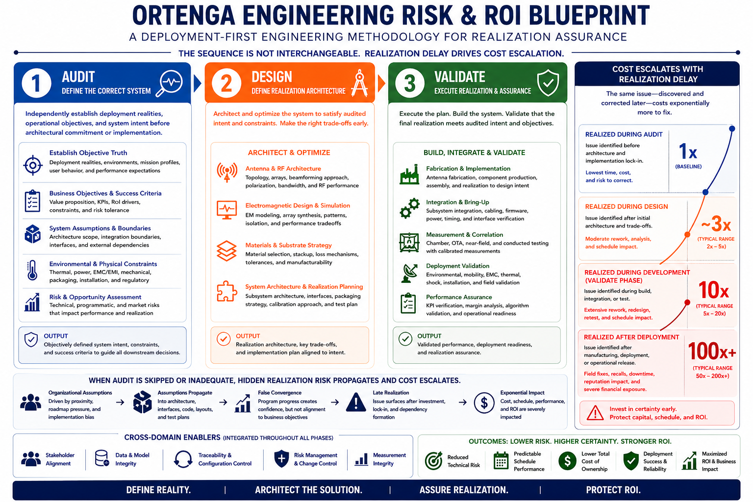
Audit
Independently establish deployment realities,
operational objectives,
manufacturability assumptions,
integration expectations,
business constraints,
and system intent before realization momentum begins.
Define the correct system and ASIC role before downstream realization risk escalates.
Design
Translate audited objectives into system architecture,
HW/FW/SW partitioning,
semiconductor allocation,
interfaces,
implementation strategy,
verification planning,
and realization architecture.
Establish realization-ready architecture before tapeout,
fabrication, and deployment validation begin.
Validate
Realize, fabricate, integrate, and verify the implementation
against deployment objectives and original system assumptions.
Confirm fabrication outcomes,
bring-up behavior,
yield integrity,
subsystem interaction,
and operational readiness.
Skipping independent upstream Audit does not eliminate realization risk.
It transfers risk downstream into architecture correction,
fabrication, integration, deployment,
schedule, and RoI exposure —
where the cost and complexity of correction increase dramatically.
Ecosystem and Adoption Risk
A technically functional architecture does not guarantee product adoption.
Successful realization also depends on identifying
the correct deployment ecosystem,
stakeholder alignment,
integration pathways,
manufacturability strategy,
and market communication approach.
Semiconductor realization extends beyond implementation success.
Long-term product viability depends on ecosystem alignment,
deployment pathways,
operational fit,
subsystem interaction,
and communicating technical value
at the appropriate system and application level.
Structured ASIC Realization Execution
Complex ASIC programs involve tightly coupled interactions
between deployment realities,
semiconductor architecture,
subsystem integration,
manufacturable hardware realization,
validation strategy,
schedule constraints,
and operational objectives.
Effective execution therefore requires structured alignment between:
- business intent
- deployment ecosystem
- system definition
- semiconductor realization architecture
- implementation execution
- fabrication and validation readiness
- operational objectives and market outcomes
Ad-hoc semiconductor execution breaks realization alignment,
increasing investment and schedule exposure
while ultimately eroding RoI.
ORTENGA operates through structured Statements of Work
designed to preserve realization alignment across architecture,
implementation, fabrication, validation,
deployment, and business objectives.
Assess ASIC Realization Risk Before Irreversible Commitments
Successful semiconductor realization is not defined solely
by implementation success.
Product success depends on whether architecture,
fabrication,
validation,
subsystem interaction,
manufacturability,
deployment objectives,
and market adoption remain aligned
throughout the complete realization lifecycle.
The objective is not simply tapeout progress.
The objective is realization alignment between deployment realities,
semiconductor architecture,
manufacturable execution,
operational validation,
and intended business outcomes.