- Split Semiconductor Wafers
- What are Pilot Test Chips and Pizza Masks?
- Transistor Semiconductor Process Selection fT, fu, fmax
- ASIC FIB
- Device Technology Push for mmW Bands
- Wafer Probe, Binning, and Wafer Map
- Delta Sigma Modulator, DSM
- Semiconductor Geometry, Moor’s Law Applicability
- HW Prototype vs. Reference Design
- Design for Manufacturability, DoM
- Design For Testability, DFT
- Shmoo Plot
- RF Amplifiers
- PLL & xCO
- DPD challenges for UWB signals
- What is Dithering and why it is used?
- What is Interleaving and Why it is used?
- Built In Self-Test, BIST
- Fractional N PLL
- PLL Requirements for Terrestrial Radio and Radar Applications
- UWB VCO
- Custom ASIC
- ASIC or Silicon Bring up
Split Semiconductor Wafers
ASIC is fundamental of many high-volume engineering solutions for commercial products.
Any product is either part of a larger system or it is actually a system.
All systems or even subsystems are comprised HW, FW, and SW.
The overall system performance is dependent on these components, HW, FW, and SW.
For a laboratory prototype device to be called an actual commercial product, it has to not only be functional but also meet specifications/system requirements over part-to-part aka process, voltage, temperature wide variations, better known as P.V.T. in the semiconductor industry.
A device that cannot handle cold or hot temperature is just a prototype, or proof of concept, and would not see commercialization daylight to return the investment.
To become commercial product, any device must be functional and meeting performance over P.V.T.
Split semiconductor wafers are intentionally altered during the engineering semiconductor fabrications in a such way that they mimic chemical variations which are typical for ASIC-to-ASIC variations of semiconductor fabrications during production phase.
The split semiconductor wafers are typically designed for at least 3 production speed variations, Slow, Nominal, and Fast.
The speed is associated with gate or transistor electron conductions performance.
Regarding RFIC, the semiconductor speed impacts gain which in turn the noise figure and non-linearity in the receiver chain. The speed impacts output power and non-linearity in the transmitter chain.
Regarding SoC, the semiconductor speed impacts the switching speed which in turn the data throughput handling of the SoC.
ORTENGA helps businesses to identify required technical features to realize their business goals.
Partner ORTENGA in your next product concept, design, and development to realize that business goal.
ORTENGA has seasoned engineering from Autonomous Automotive, SATCOM, radar, Smart City, and Mobile Terrestrial Radio Communications System industries in ASIC, HW, FW, and SW engineering disciplines.
What are Pilot Test Chips and Pizza Masks?
Application Specific Integrated Circuits, aka ASIC, are high volume electronic circuits which provide functionality of some portion of communications and/or radar systems. One of major cost components of these ASIC, is semiconductor mask. Semiconductor masks are used for lithographically fabricating the semiconductor devices onto wafer. Each wafer requires multiple masks for various layers of fabrications and etching. A typical vanilla CMOS process could easily have 200 masks or more and they could easily cost as much ~$3M depending on the geometry and size of the gates.
Each all layer revisions of ASIC require all ~200 masks; therefore it becomes prohibitively expensive for smaller companies or even big corporations to tape out any design for single project/product.
In order to save cost for any trial of ASIC before design is finalized, it is customary to run some pilot test chips to validate the design as well as the process performances. For test chips run, it should only be enough number of them to be validated and characterized for desired performances, KPI.
Therefore, many semiconductor fabrications offer Pizza Mask, where number of companies can share the cost for the masks, ~$3M, and get only small portion of wafer area, “pizza”. Very large corporations typically have their own pizza masks for multiple internal projects, test chips. Or tandem with another project masks for couple hundred devices.
Each wafer lot is typically 25 wafers, and small portion of pizza/wafer, can produce few hundred devices per lot, enough to validate design topology and performance metrics.
Augment ORTENGA in your semiconductor device design and developments to utilize cost saving proven techniques which are not only benefits R&D cost, but also improves TTM, hence ROI.
Device Technology Push for mmW Bands
CMOS technology has been the technology of choice for baseband digital and mixed signaling for number of decades. In that past decade, CMOS was utilized for some of RF transceivers.
As radio transceivers go into mmW bands, the use of CMOS for RF signaling becomes limited and III-V compound technology are required to meet the specifications. The following chart illustrates the Maximum Stable Gain, MSG comparison for CMOS vs. III-V compound technologies over the next few years.
ORTENGA has seasoned engineering from Autonomous Automotive, SATCOM, radar, Smart City, and Mobile Terrestrial Radio Communications System industries in ASIC, HW, FW, and SW engineering disciplines.
Transistor Semiconductor Process Selection fT, fu, fmax
fT, Transition frequency is the transistor highest frequency where the current gain is unity or 0 dB, beyond this frequency there is no current gain.
fmax, maximum frequency is the transistor highest frequency where the unilateral gain becomes unity or 0 dB, beyond this frequency there is no power gain.
Many useful circuits require either current, voltage, or power gain.
As the application of radio frequencies increases, the required transistor’s fT increases too.
For given semiconductor process, the gain slop is negative with 6dB/Octave or 20dB/decade in frequency.
Silicon processes’ fT is a technical driver and depending on required “gain” or applicability a process is down-selected.
Obviously, cost is another driver for down-selecting the semiconductor process.
The cost of wafer drives the cost of ASIC.
The cost of wafer depends on the size of the wafer, the semiconductor process, and the number of lithography masks, which together drive the die per wafer cost.
As the wafer size increases, the number of dies per wafer increase, therefore ASIC cost decreases.
The silicon wafers, CMOS process in particular could be as large 15” diameter nowadays.
Higher radio frequencies’ circuitry requires III-V compound semiconductor process with higher fT, such as GaAs, GaN, InP, etc.
The III-V wafers could be as large as 8” diameter nowadays and they are fewer fabs that can develop them.
The III-V compound semiconductors are typically used for applications with high RF performance which are less cost sensitive, such as; advance radio, radar, space, or specialized and custom-made radio front ends.
Furthermore, ASIC cost depends on wafer yield, wafer probe test time, packaged ASIC test time, and the package itself which could be significant portion of the total cost.
The wafer yield impacts the cost of ASIC and depends on circuit design topology and implementations as well as selected process tolerances.
Partner ORTENGA to succeed in your design and product delivery to the market.
ORTENGA has seasoned engineering from Autonomous Automotive, SATCOM, radar, Smart City, WiFi, and Mobile Terrestrial Radio Communications System industries in Antenna, ASIC, Algorithm, HW, FW, and SW engineering disciplines.
ASIC FIB
ASIC design and development go through multiple design reviews from early stage until tapeout.
During tapeout schematic vs. layout should be compared and any discrepancy should be carefully resolved.
Still, there are miscommunications and simple overlook occur.
These errors cause functionality at most and sometime performance issues only.
Functionality issues are the one where the circuit does not function at all.
Whereas performance issues are the one where the circuit functions yet do not meet all some performance metrics.
Functionality issues prevent any evaluation of the circuit.
Given ASIC tapeout expenses and timeline to fix any functional issue, there could be alternative option, FIB.
Focused Ion Beam, FIB allows to alter some changes to top layer of silicon for debugging and testing.
The easiest changes are to the metal layer connectivity.
ORTENGA helps businesses to identify required technical features to realize their business goals.
Partner ORTENGA in your next product concept, design, and development to realize that business goal.
ORTENGA has seasoned engineering from Autonomous Automotive, SATCOM, radar, Smart City, WiFi, and Mobile Terrestrial Radio Communications industries in Antenna, ASIC, HW, FW, and SW engineering disciplines.
Wafer Probe, Binning, and Wafer Map
Semiconductor wafers go through a long and costly expenses to be developed during production phase of any wafer lot.
The turn-around time is typically anywhere between 30 to 60 days depending on the process and fab house.
After the completion of the wafer lot, they go through wafer probe for design and process validations.
This testing occurs with Automatic Test Equipment, ATE which are similar to robot with testing capabilities.
Each wafer has thousands of Dies, i.e. ASIC, which would be tested individually.
A good die would pass all expected wafer test, Bin 1.
On the other hand, the bad dies are binned for various failures.
For instance, a die may fail for merely parametric of a single parameter marginally, Bin 2, while another die fails simple drawing current, Bin 99.
An electronic record of these failures with various bin numbers will be saved and called Wafer Map and will be passed on to the next step.
The next step is wafer dice and sort each bin number separately.
Obviously, Bin 1 Dies will be used for packaging.
Other Bins have to be analyzed if improving yield or root cause analysis is desired.
The yield impacts the cost of die per wafer.
ORTENGA has seasoned engineering from Autonomous Automotive, SATCOM, radar, Smart City, WiFi, and Mobile Terrestrial Radio Communications System industries in Antenna, ASIC, Algorithm, HW, FW, and SW engineering disciplines.
Delta Sigma Modulator, DSM
Ultra wide bandwidth data converters, ADC and DAC are becoming required for many applications, such as; advanced radio communications and radar systems.
UWB data converters enable monitoring/generating multiple signals within the overall system whether that is radio communications or radar applications.
In radio communications, the faster response time translate to shorter processing time for multiple signals.
In radar, the faster response time translate to shorter time to be aware of multiple targets.
DSM architecture can be configured for high resolution and low noise for UWB applications.
ORTENGA works with client and stakeholders to identify goals and deliverables of the project.
ORTENGA helps businesses to identify required technical features to realize their business goals.
Partner ORTENGA in your next product concept, design, and development to realize that business goal.
ORTENGA has seasoned engineering from Autonomous Automotive, SATCOM, radar, Smart City, WiFi, and Mobile Terrestrial Radio Communications System industries in Antenna, ASIC, Algorithm, HW, FW, and SW engineering disciplines.
Semiconductor Geometry, Moor’s Law Applicability
Digital circuitry relies on switching transistors, binary logic, 0 and 1.
Switching technology is directly proportional to semiconductor geometry.
Therefore, by reducing the geometry, the switching technology shrinks.
The size reductions have two impacts, the cost by increasing die per wafer, as well as reducing sleep current/power consumption.
Waveform generation and waveform analysis occur in digital circuits.
DSP is implemented by digital circuits with FPGA or equivalent processor.
The actual information is embedded in the digital waveform.
Analog circuitry, in particular, RF circuits are comprised of capacitors, inductors, as well as amplifiers.
It is only the amplifiers which utilize transistors and are relatively few comparing to digital circuits.
The inductance and capacitance values depend on semiconductor/silicon area and relative dielectric and permeability constants therefore their size does not scale with semiconductor geometry.
In reality the RF circuits scale with wavelength (frequency), therefore at operational frequencies the RF circuitry is small portion of the overall system, i.e., Digital, Mixed Signal, Analog circuits.
It is only signal conditioning and integrity of EM waves (carrier) which occur in the RF circuits.
ORTENGA helps businesses to identify required technical features to realize their business goals.
Partner ORTENGA in your next product concept, design, and development to realize that business goal.
ORTENGA has seasoned engineering from Autonomous Automotive, SATCOM, radar, Smart City, WiFi, and Mobile Terrestrial Radio Communications industries in Antenna, ASIC, HW, FW, and SW engineering disciplines.
What are the differences between HW Prototype and Reference Design?
There are two types of HW projects; first Prototype, second Reference Design.
They are both similar yet with somewhat different objectives.
In case of HW Prototype, although there is some analysis and simulation, but the functionality and performance of the HW has never been verified.
This typically applies to out of box and innovative ideas and design validation which is required. HW Prototype is also used to characterize the design/device over Process, Voltage, and Temperature, aka PVT.
On the other hand HW reference design implies that there is confidence and supporting PVT data on the performance of the design, via HW Prototype.
The HW reference design is final product that external customer can acquire and validate them on their own.
The HW reference design is sometimes called the Evaluation Kit, aka Eval Kit.
Customer gets Gerber and Schematic files as well as design guidelines for duplicating the reference design.
Partner with ORTENGA in your HW design, development, and Bring up.
ORTENGA helps businesses to identify required technical features to realize their business goals.
Partner ORTENGA in your next product concept, design, and development to realize that business goal.
ORTENGA has seasoned engineering from Autonomous Automotive, SATCOM, radar, Smart City, WiFi, and Mobile Terrestrial Radio Communications industries in Antenna, ASIC, HW, FW, and SW engineering disciplines.
Design for Manufacturability, DoM
In general, any electronic circuit performance varies across Process, Voltage, and Temperature, PVT.
Process being circuit to circuit variations due to components’ tolerances, another words, part to part variations.
Applied voltage variations can impact the circuit performance.
Needless to say, temperature impacts the outcome of everything in the nature.
Furthermore, for RF circuits have frequency dependence.
Any manufacturable product must meet the product requirements over PVT.
Any device or product which does not meet the requirements, is technically not reproducible and failing devices would be returned by its customers.
That’s what differentiate a product from a prototype.
Prototype is not necessarily reproducible in volume, but demonstrates the concept behind its design.
Many companies fall into prototype which are not reproducible and cannot return the investment.
Partner with ORTENGA in your HW design, development, and Bringup.
ORTENGA helps businesses to identify required technical features to realize their business goals.
Partner ORTENGA in your next product concept, design, and development to realize that business goal.
ORTENGA has seasoned engineering from Autonomous Automotive, SATCOM, radar, Smart City, WiFi, and Mobile Terrestrial Radio Communications industries in Antenna, ASIC, HW, FW, and SW engineering disciplines.
Design For Testability, DFT
While testing any ASIC product occurs at the end of manufacturing cycle, the test could have far more implications on the return of the investment than originally planned.
A successful ASIC product which returns the investment has to meticulously budgeted for cost of every phase of its life cycle.
ASIC life cycle can be comprised of, product concept, ASIC requirements, design, manufacturing, and test.
Testing ASIC is the very last step in manufacturing before ASIC is shipped out the door, yet if testing methodology and requirements are not considered during the product concept, it could cost more or triggers many returns by the customers.
ASIC test cost is significant portion of overall budget and has to be carefully monitored.
To reduce the AISC cost and increase margin, the testing capability has to be studied and designed in such a way that it minimizes the testing time.
Minimizing ASIC test time is a challenging task which puts technical requirements on the ASIC design.
Design For Testability, DFT applies to highly complex ASIC which return the investment by taking into account testing methodology right up front in the design phase.
Many companies which did not integrate for DFT in their product life cycle, have fallen short in returning the investment.
Partner with ORTENGA in your HW design, development, and Bringup.
ORTENGA helps businesses to identify required technical features to realize their business goals.
Partner ORTENGA in your next product concept, design, and development to realize that business goal.
ORTENGA has seasoned engineering from Autonomous Automotive, SATCOM, radar, Smart City, WiFi, and Mobile Terrestrial Radio Communications industries in Antenna, ASIC, HW, FW, and SW engineering disciplines.
Shmoo Plot
Digital ASIC can be characterized at early stages for their performances, wafer probe via ATE.
The metrics of interest are functionality of logic gates over clock speed and Vcc.
The Shmoo plot is a quick health metric of digital ASIC.
ASIC performance can be done at various location on the silicon wafer or over various wafers to gain confidence on the measured data and statistical yield.
By tweaking some of the parameters, additional performance may be achieved.
The test stimuli for driving the digital ASIC are typically known as the test vector.
Test vector generation requires understanding not only the ASIC functionality but also designing appropriate vector and validating them before ASIC becomes available.
Time is of essence for commercial ASIC market to return the investment at an appropriate margin, therefore the sooner the ASIC is characterized and ready for production, the wider the margin.
Partner with ORTENGA in your HW design, development, and Bringup.
ORTENGA helps businesses to identify required technical features to realize their business goals.
Partner ORTENGA in your next product concept, design, and development to realize that business goal.
ORTENGA has seasoned engineering from Autonomous Automotive, SATCOM, radar, Smart City, WiFi, and Mobile Terrestrial Radio Communications industries in Antenna, ASIC, HW, FW, and SW engineering disciplines.
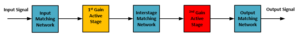
RF Amplifiers
RF amplifiers are used both in radio transmitter and receiver chains.
In the transmitter, there are two amplifiers, Drive Amplifier, DA and Power Amplifier, PA.
DA is typically post transceiver yet before PA, hence Drive Amplifier.
PA is the last amplification stage before the signal is delivered to antenna.
The objectives of both DA and PA are to amplify and increase the signal to adequate level before transmission into the air.
In the receiver chain, there are also at least two stages of amplifications.
Low Noise Amplifier, LNA is the closed amplifier to the antenna. It is function is to amplify the small incoming signal yet at add very small amount of thermal noise.
It is less known to many that every electronic circuit add some noise to the signal and reduces SNR. That applies to amplifiers too.
Trans-Impedance Amplifier, TIA is another amplifier typically after the frequency conversion and before ADC. TIA could be known as IF amplifier.
Regardless of amplifier function, they are typically comprised of transistors active device for providing gain as well as input and output matching network.
What differentiate all of the above amplifiers, are two things.
First the transistor selected for gain or amplification.
Second the input and output matching network objective.
While the name may suggest the matching network job is to match the impedance.
The reality is different.
The matching network for LNA is noise match, while for PA is to power match.
In both cases the matching network is supposed to their job while keeping the circuit stable.
The stability is unspoken constraints yet implied and perhaps the most important requirement for any amplifier is to amplify not oscillate.
Typically, each gain stage can provide by up to 10dB gain, therefore multiple gain stages are needed to have larger gain amplifier.
Partner with ORTENGA in your HW design, development, and Bringup.
ORTENGA helps businesses to identify required technical features to realize their business goals.
Partner ORTENGA in your next product concept, design, and development to realize that business goal.
ORTENGA has seasoned engineering from Autonomous Automotive, SATCOM, radar, Smart City, WiFi, and Mobile Terrestrial Radio Communications industries in Antenna, ASIC, HW, FW, and SW engineering disciplines.
PLL & xCO
Phased Locked Loop, PLL and Voltage Control Oscillator, VCO are part of any ASIC whether it is analog, mixed signal, or digital circuits.
PLL and VCO provide Local Oscillator, LO functionality for any legacy Heterodyne and Homodyne radio front end.
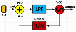
PLL and Numerical Control Oscillator, NCO provide clock functionality for mixed signal and digital circuits.
In radio front end the PLL and VCO phase noise contribute to noise budget and overall RF impairments of the radio which impact SNR.
Poor phase noise could desensitize and/or reduce dynamic range of the receiver.
Aperture jitter impacts Software Defined Radio, SDR SNR.
Jitter is time domain signature of phase noise in frequency domain.
ORTENGA helps businesses to identify required technical features to realize their business goals.
ORTENGA is comprised of seasoned and skillful engineers who collaborate on innovative design in entrepreneurial environment to accomplish clients’ project.
Partner ORTENGA in your next product PLL ASIC design and development to realize that business goal.
ORTENGA has seasoned engineering from Autonomous Automotive, SATCOM, radar, Smart City, WiFi, and Mobile Terrestrial Radio Communications industries in Antenna, ASIC, HW, FW, and SW engineering disciplines.
DPD challenges for UWB signals
Digital Pre Distortion, DPD, technique is widely used in mobile UE to linearize Power Amplifier, PA, output signal, such that it can be run into saturation mode without violating spurious and unwanted emissions while mitigating transmitter power efficiency, hence increasing the battery life time.
It turns out that spectral efficiency and power efficiency have contradictory constraints.
As we pack more bits into one symbol or alphabet, higher QAM, then the signal becomes more spectral efficient, bit per second per Hz, bps/Hz, hence more throughput. As a result, the Peak power to Average Ratio, PAR, between each symbol can change significantly. Higher PAR requires higher linearity PA, which in turns requires higher power consumption, hence less power efficiency.
5G is targeting higher BW or user datarates; up to 100MHz for FR1 and up to 4GHz for FR2 bands.
DPD techniques are based on pre distorting the desired signals prior to feeding in to the PA in such a way that the output is linear, i.e. the output is amplified version of the PA input signal. This is possible when PA characteristic is well known in terms of AM2AM and AM2PM and utilized to predistort the desired input signal and feasible when PA characteristic is memoryless.
Memoryless refers to the fact that the output of PA does not depend on the previous input samples, only on the current sample. PA can be memoryless up to a critical BW, which turns out to be around 20MHz. In other words, PA is forgiving for less than 20MHz signal BW and has memory for signals over 20MHz.
For UWB, e.g. 5G mmW signals, DPD algorithms become run time computations. That implies there is control loop which looks at the input and output signal of the PA and makes appropriate predistortion for every symbol to be transmitted. The DPD control loop bandwidth becomes excessively large as the signal BW increases.
The following diagram illustrates the output of typical PA.
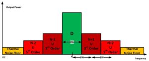
It can be seen that the first upper and lower adjacent channels are 3rd order intermodulation, whereas second upper and lower adjacent channels are 5th order intermodulation of the desired signal. DPD job is to reduce these 3rd and 5th order intermodulation terms, significantly.
That implies, DPD has to have control loop bandwidth in such a way to resolve the first and second adjacent channels in frequency, total 5x BW. By Nyquist sampling theorem that implies 10x BW of desired signal is required for DPD control loop.
Here is the summary of DPD challenges for 5G application, UWB:
- Memory effect of PA
- Run Time DSP computations of Predistortion signals
- Control Loop BW of DPD
The question becomes, are there alternative ways to linearize the PA output?
Partner with ORTENGA in system design and development.
What is Dithering and why it is used?
Dithering is a technique of reducing spurious unwanted signal which are unavoidable due to design architecture.
By modulating the unwanted spurious signal with wide band noise, the spurious signal can be reduced by several dB and in some cases suppressed below noise floor.
It is analogous to putting out fire by fire.
Dithering has applications in PLL, DSM, ADC, and DAC where spurious signals are number of one challenge for operational success.
Partner with ORTENGA for your PLL, DSM, ADC, and DAC design and development.
What is Interleaving and Why it is used?
Interleaving is the process of placing/shuffling bits within a symbol in such a way that decrease the chance of “Burst Errors” due to fading.
There are two class of interleaving, Block and Convolutional.
Block interleaving is when the symbol is written into row of a matrix and transmitted along the column of that matrix.
Pseudorandom Block interleaving is subclass and when the symbol is written into row of a matrix and transmitted in the pseudorandom mechanism.
Convolutional interleaving is when the symbol is multiplexed in and out of fixed number of shift registers.
Partner with ORTENGA to design and develop your new product.
Built In Self-Test, BIST
As integration level increases, not only testing methodology becomes more challenging, but also the cost of testing vs. scrapping components becomes prohibitive for volume production.
Built in self-test, BIST allows each major block to be designed for self-test and validation during manufacturing or even operations.
BIST is proactive methodology which takes into account the production cost as well as smooth operations.
BIST is applicable to PLL, Tx chain, Rx Chain, ADC, DAC, Antenna installation versification, Fault isolation, etc.
Partner with ORTENGA to design and development for your new product BIST.
Fractional N PLL
Phased Lock Loop, better known as PLL are used to generate Local Oscillator, LO for radio front end or Clock for baseband circuitry.
Clock to ASIC is similar to Heart to Body which drives and organize timing responses of various organs. Without Heart, the body cannot function, without Clock the ASIC cannot function.
Fractional N PLL aka Frac N PLL has 3 main advantages over Integer N PLL.
- Finer step frequency resolution relative to reference frequency
- One Frac N PLL can provide LO function for both Tx and Rx chain
- Agility to perform digitally controlled modulation
Needless to say, the above advantages do not come free, the Frac N PLL is much more complex in design and development.
In spite of that, the advantages overcome the trade off and are attractive in advanced ASIC.
Partner with ORTENGA to design and develop PLL ASIC.
PLL Requirements for Terrestrial Radio and Radar Applications
PLL phase noise requirements are driven by in band, IB and out of band, OOB drivers.
IB driver is dominated by desired channel purity requirements which has budget in overall SNR.
OOB driver is dominated by adjacent channel, typically considered undesired, which has budget in dynamic range of the system.
Dynamic Range, DR of a radio is measure of how the radio can handle both small desired signal in presence of loud unwanted signal.
SNR and DR of any system whether it is Terrestrial Radio or Radar are of significant concern and differentiators for end users.
Partner with ORTENGA to design and develop PLL ASIC.
UWB VCO
Ultra-Wide Band, UWB VCO are required in mmW and Radar applications.
Single VCO bandwidth circuitry is similar single element antenna bandwidth and can be quantified between 5 -10 % fractional bandwidth, FBW.
To increase the absolute bandwidth, the VCO frequency can be increased to 2x, 4x, or 8x of the required center frequency.
Consequently, post LO is frequency divided version of VCO.
Effectively that reduces the number of VCO for pulling full frequency range in UWB application, hence smaller ASIC die size, i.e., lower cost.
Octave or its multiple octave VCO resonance frequency helps with LO spurious free or purity of the desired spectrum.
These VCO provide mmW PLL functionality for mmW and Radar applications.
Partner with ORTENGA for frequency planning of UWB mmW and radar systems and VCO design and development.
Custom ASIC
ORTENGA has ASIC design and development capabilities now, in addition to Antenna and Algorithm design and development.
A radio communications or radar system has four major functional blocks, namely Antenna System Module, ASM, Front End Module, FEM, Transceiver Module, TRM, and Baseband Module, BBM.
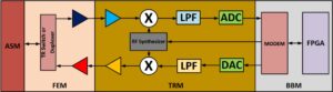
Some of the mentioned blocks could be integrated into adjacent block or completely eliminated by choosing alternative architecture. Nevertheless, a large number of legacy systems follow the above architecture. ORTENGA tailors the above architecture to the client’s requirements for their application.
Historically, ORTENGA started with system architecture and definitions.
Then, ORTENGA enhanced its Algorithm development portfolio.
Typically, algorithms reside in FPGA.
ASM, FEM, and TRM functions are signal conversion and maintain signal integrity, whereas BBM function is to generate outgoing signals or detect and decipher the incoming signals within the MODEM.
Now, ORTENGA provides ASIC services for clients, either as a particular IP which can be integrated by the client into an IC or design and developing complete ASIC.
Over the past decade has grown and has end to end system design and development capability which can be tailored to many applications, such as; Autonomous Automotive, Radar, Smart City.
Partner with ORTENGA for design and development of your custom IP or ASIC that is tailored for your new product using seasoned engineering network.
ASIC or Silicon Bring up
Design and development of ASIC from concept to actual product goes through many phases.
Each phase requires specialized engineering skills that are challenging and takes considerable time to master.
Silicon or ASIC bring up phase to verify the design’s goal is no different.
Having silicon is not equivalent to having a prototype yet alone a product that can be manufactured in high volume for commercial applications.
Partner ORTENGA in design and development of your ASIC and silicon bring up to expedite time to market of your product and harvesting the return of the investment.